Saturday 10 November 2012

MPPT CIRCUIT


List of Components

No.
Component
Quantity

Preset
1
10k
1 pcs

Capacitor
2
100nF (ceramic)
3 pcs

Diode
3
4148
2 pcs
4
IN 5818
1 pcs

IC
5
NE555
1 pcs
6
IC base (8 pin)
1 pcs

Inductor
7
Toroid
1 pcs

Mosfet

8
IRFZ44N
1 pcs


PCB design by using Design Spark Software


3D top preview


 3D bottom view


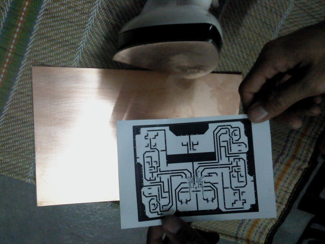
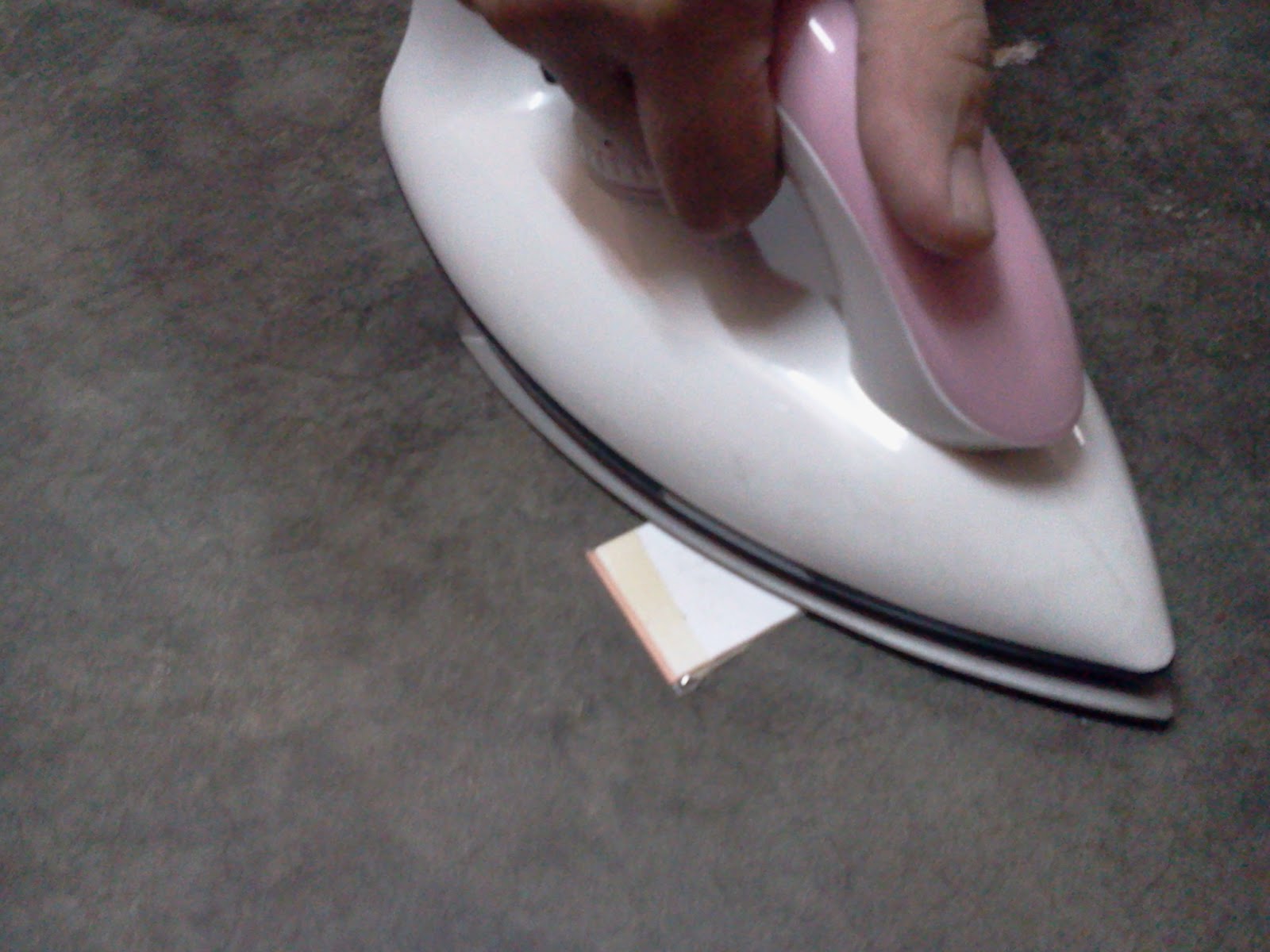
1) Print the PCB layout on the gloss paper / photo paper by using laser jet printer.Place the photo paper face down on the copper clad board.Use a hot clothes iron to transfer the track pattern from the paper to the copper board. 


2) Put the board in the acid solution (Ferric Chloride) and agitate until the unwanted copper traces are completely etched.


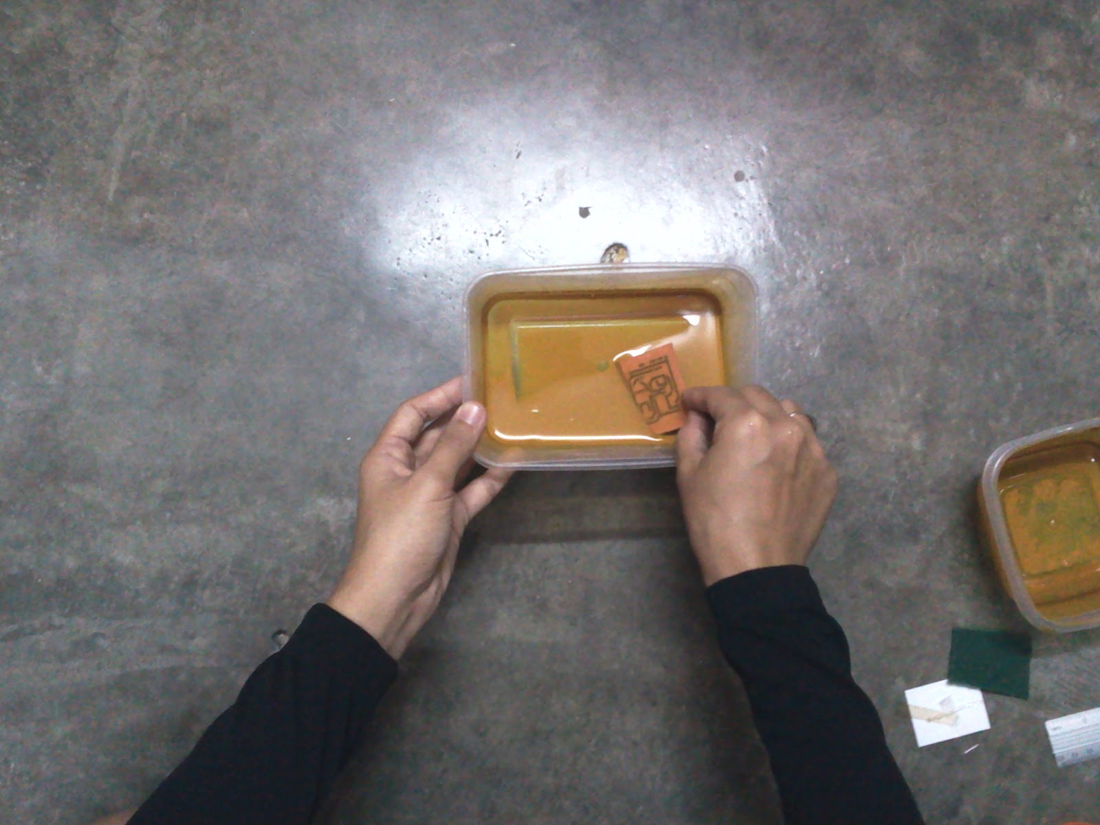
3) Rinse the board with a tap water and dry it. Dissolve the printed toner with paint thinner.


4) Drill holes (holes should be at least 0.1 mm bigger than pins / wires) 


5)  Put the component at proper place and solder it. 


Circuit Design


 List of Components
No.
Component
Quantity

Resistor
1
1k
4 pcs
2
15k
8 pcs

Preset
3
10k
6 pcs

Capacitor
4
100nF (ceramic)
32 pcs
5
470uF 16V (electrolytic)
1 pcs
6
10uF 16V(electrolytic)
1 pcs
7
1uF 16V (electrolytic)
2 pcs

Diode
8
4148
4 pcs
9
IN 5818
8 pcs

IC
10
NE555
2 pcs
11
TLC 3702
2 pcs
12
IC base (8 pin)
4 pcs

Voltage regulator
13
L7805
1 pcs


PCB design by using Design Spark Software


3D top preview

 3D bottom view


1) Print the PCB layout on the gloss paper / photo paper by using laser jet printer.


2) Then rub the PC board surface by using scouring pad until the oxidised layer cleaned.


3) After that, clean the PC board surface with paint thinner until oxidised dust totally clean.


4) Place the photo paper face down on the copper clad board.


5) Use a hot clothes iron to transfer the track pattern from the paper to the copper board. Then cut the board suits designed layout.


6) Put the board in the acid solution (Ferric Chloride) and agitate until the unwanted copper traces are completely etched.


7) Rinse the board with a tap water and dry it.


8) Drill holes (holes should be at least 0.1 mm bigger than pins / wires) 


9) Dissolve the printed toner with paint thinner.


10) Put the component at proper place and solder it.